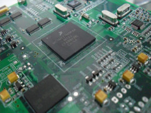
There is an element of art and science in the design and placement of components on a printed circuit board. There are rules that guide the electronic placement of individual components. However, the art of operationalizing the board is what will determine its quality and performance. Experts at PCB assembly service have identified five tips that will make your placement of components on the board perfect to produce a function and efficient board.
1. Consider Your Mechanical Ability
Mechanical constrains refer to the placement of your mounting holes and where the edge connectors go. You should also consider the type of enclosure you will be using for your board. These are the variables that will have a direct impact on the shape and size of your Board. By making prior considerations, you will avoid incidences where the board fails to fit in its enclosure. In such a case, you are forced to spend more hours reworking on the board. When you have cleared with your mechanical capability, you have time To pay attention to your creative aspects of building the board.
2. Assembly Capabilities
There are assembly plants that expose the Edges of your board to damage. Others are meticulous and do not present any threat. When these considerations are made, you will generate a board that meets your expectations and is not prone to damage on the edges during assembly or when it is being operated.
3. Breathing Room For Integrated Circuits (IC )
The allowance that should be provided is 0.3”-0.5” between one integrated circuit and the other. If you are dealing with larger circuits, the space should be increased. This space is asked to allow pins to come in and leave the circuit. Without Adequate space, you are likely to run out of space during routing. This means that you will have to review your design, a process that takes time and resources. The movement of components at this point will destroy the aesthetics of your board.
4. Similar Components Should Be Kept In The Same Direction
Will a wider view of your board where components that perform the same function are kept in a row or column. this makes it easier to organize your board. The board will also be neat. Installation, inspection and testing of the board will also be easier .
5. Minimize Connection Paths By Grouping
The professional way is to ensure that paths do not intersect or crisscross. This is done to make routing easier and also allow you to use fewer connections. Modern design software provides the most efficient paths to these solutions.
About Agile Circuit
Agile Circuit provides the most professional and efficient PCB assembly service. You get a comprehensive package that includes design, assembly, testing and operationalization. With experts in printed circuit boards, you are guaranteed the most efficient board for your operations.

