Multi-layer PCBs are circuit boards made up of more than two electrical layers (copper layers) superimposed on each other. The copper layers are bonded together by resin layers (prepreg). Multi-layer boards represent the most complex type of printed circuit boards. Their cost is relatively high, owing to the complexity of the manufacturing process, lower production yields and difficulty of re-working on them. The need for multi-layer boards has been necessitated by the increasing packaging density of integrated circuits, which give rise to a high concentration of interconnecting lines.
Why do we need Multi-layered PCBs?
The printed circuit layout results in unpredictable design problems like noise, stray capacitance, cross-talk etc. The PCB design, therefore, must aim at minimizing the length of the signal lines and avoiding parallel routing etc. Obviously, such type of requirements could not be met satisfactorily in single-sided and even double-sided printed circuit boards due to limited cross-over which could be realized. Thus, to achieve satisfactory performance from the circuit in the presence of a very large number of interconnections and cross-over, the PCB must be extended beyond two-plane approach.
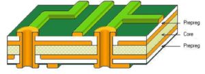
This gives rise to the concept of multi-layer circuit boards. Hence, the primary intent of fabricating a Multilayer printed circuit board is to provide one more degree of freedom in the selection of suitable routing paths for complex and/or noise-sensitive electronic circuits. Multi-layer boards have at least three layers of conductors, in which two layers are on the outside surface while the remaining one is incorporated into the insulating boards. The electrical connector is commonly completed through plated through-holes, which are transverse to the boards. Unless otherwise specified, Multi-layer PCBs are assumed to be plated through hole as with double-sided boards.
Multi-layer boards are fabricated by stacking two or more circuits on top of each other and establishing a reliable set of pre-determined interconnections between them. The technique begins with a departure from conventional processing in that all the layers are drilled and plated before they are laminated together. The two innermost layers will comprise conventional two-sided PCB while the various outer layers will be fabricated as separate single-sided PCBs.
Prior to lamination, the inner layer boards will be drilled, plated through, imaged, developed and etched. The drilled outer layers, which are signal layers, are plated through in such a way that uniform donuts of copper are formed on the underside rims of the through-holes. This is followed by lamination of the various layers into a composite multi-layer with wave-solderable interconnections.
The lamination may be performed in a hydraulic press or in an overpressure chamber (autoclave). In the case of hydraulic press, the prepared material (press stack) is placed in the cold or preheated press (170 to 180 °C for material with a high glass transition point). The glass transition temperature is the temperature at which the amorphous polymers (resins) or the amorphous regions of a partially crystalline polymer change from a hard and relatively brittle state to a viscous, rubbery state. Multi-layer boards find applications in professional electronics (computers, military equipment), particularly whenever weight and volume are the over-riding considerations.
However, there has to be a trade-off which is simply the cost of space and weight versus the board’s costs. They are also very useful in high-speed circuitry because more than two planes are available to the PCB designer for running conductors and providing for large ground and supply areas.